

Press-Fit Assembly: A Path to High-Reliability Interconnect
Press-fit is a solderless PCB assembly process. Special elastic terminals are pressed into plated through-holes so that controlled plastic deformation creates a gas-tight electrical connection. The process is evaluated under IEC 60352-5 and is widely used in high-reliability applications.
From Soldering to Press-Fit
Soldering relies on molten tin alloy to diffuse metal atoms and form a joint. Press-fit changes the logic entirely: at room temperature, mechanical force alone creates intimate contact between the terminal and the hole wall.
As electronics move toward finer pitch and higher pin counts, traditional soldering becomes harder to control, while press-fit has become a key technology for high-density assembly.
Key Advantages
1. Avoid soldering defects and improve yield
Press-fit eliminates cold joints, insufficient wetting, solder balls, poor hole fill and solder bridges. Without heat, PCBs and nearby sensitive components are free from thermal stress—especially valuable on thick multilayer boards.
2. Simplify process and lower total cost
Removing soldering reduces solder/flux consumption, cleaning steps and downtime. Connectors often need no extra screw fastening after press-fit, further simplifying assembly.
3. Reworkability and design flexibility
Within rated cycle limits, press-fit connectors can be reworked. Terminals can be used on both PCB sides, supporting mixed PTH/SMT layouts and higher routing density.
4. Suitable for high-speed / high-frequency designs
Stable contact resistance and strong HF behavior make press-fit a fit for multilayer, miniaturized high-speed signal designs.
Quality Prerequisites
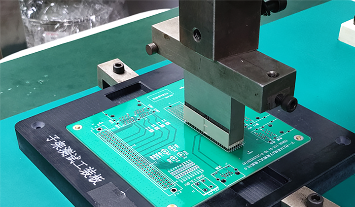
Reliability depends on three factors working together: elastic terminal design (e.g. eye-of-needle), application-specific tooling, and precision press equipment. Industry practice typically keeps effective insertion force per pin within about 35 N to avoid connector deformation or PCB damage.
Typical Applications
AI servers and data-center high-speed backplanes, automotive electronics (navigation, xEV drivetrains, ADAS), rail signaling backplanes, aerospace/defense (VPX, avionics), and telecom base-station backplanes.